1998 TCAD-assisted analysis of back-channel leakage in irradiated mesa SOI nMOSFETs
реклама
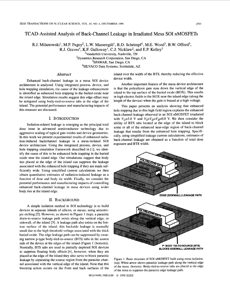
IEEE TRANSACTIONS ON NUCLEAR SCIENCE, VOL. 45, NO. 6, DECEMBER 1998 2593 TCAD-Assisted Analysis of Back-Channel Leakage in Irradiated Mesa SO1 nMOSFETs R.J. Milanowski', M.P. Pagey2, L.W. Massengill', R.D. Schrimpf', M.E. Wood3, B.W. Offord3, R.J. Graves4, K.F. Galloway', C.J. Nicklaw2, and E.P. Kelley3 'Vanderbilt University, Nashville, TN 2Dynamics Research Corporation, San Diego, CA 3SPAWAR, San Diego, CA 4SILVAC0 Data Systems, Scottsdale, AZ Abstract Enhanced back-channel leakage in a mesa SO1 device architecture is analyzed. IJsing integrated process, device, and hole trapping simulation, the cause of the leakage enhancement is identified as enhanced hole trapping in the buried oxide near the island edge. Simulation results suggest this edge effect may be mitigated using body-tiled-to-source tabs at the edge of the island. The potential performance and manufacturing impacts of this measure are discussed. I. INTRODUCTION Isolation-related leakage is emerging as the principal total dose issue in advanced semiconductor technology due to aggressive scaling of typical gate oxides and device geometries. In this work we present experimental results of enhanced radiation-induced backchannel leakage in a mesa-isolated SO1 device architecture. Using the integrated process, device, and hole trapping simulation framework described in [l], we identify the cause of this to be enhanced hole trapping in the buried oxide near the island edge. Our simulations suggest that body ties placed at the edge of the island can suppress the leakage associated with the enhanced hole trapping if they are made sufficiently wide. Using simlplified current calculations we then obtain quantitative estimates of radiation-induced leakage as a function of dose and body tie width. Finally, we consider the potential performance and manufacturing impacts of controlling enhanced back-channel le,skage in mesa devices using wider body ties at the island edge. II. B l ~ A simple isolation method in SO1 technology is to build devices in separate islands of silicon, or mesas, using anisotropic etching [2]. However, as shown in Figure 1 (top), a parasitic drain-to-source leakage path exists along the vertical edge, or sidewall, of the island [3]. A leakage path also exists on the bottom surface of the island, this backside leakage is normally small due to the high threshold voltage associated with the thick buried oxide. The edge leakage path can be suppressed by creating narrow p-type body-tied-to-source (BTS) tabs in the source side of the device at the edges of the island (Figure 1 (bottom)). Normally, BTS tabs are used in partially depleted SO1 devices to suppress floating body effects [4], however, when they are placed at the edge of the island they also serve to block parasitic leakage by separating the source region from the parasitic channel associated with the vertical edge of the island. Note that this blocking action occurs on the front and back surfaces of the 0018-9499/98$10.00 island over the width of the BTS, thereby reducing the effective device width. Another important feature of the mesa device architecture is that the polysilicon gate runs down the vertical edge of the island to the top surface of the buried oxide (BOX). This results in high electric fields in the BOX near the island edge (along the length of the device) when the gate is biased at a high voltage. This paper presents an analysis showing that enhanced hole trapping due to this high field region explains the enhanced back-channel leakage observed in an SO1 nMOSFET irradiated with V ~ = 5 . 0V and Vs=VD=VB=O.O V. We then consider the ability of BTS tabs located at the edge of the island to block some or all of the enhanced near-edge region of back-channel leakage that results from the enhanced hole trapping. Specifically, using simplified leakage current calculations, estimates of back-channel leakage are obtained as a function of total dose exposure and BTS width. ~ ~ ~ ~ BLOCKS SIDEWALL LEAKAGEPATH Figure 1. Basic structure of SO1 nMOSFET built using mesa isolation. (top) White arrow shows parasitic leakage path along the vertical edge of the mesa. (bottom) Body-tied-to-source tabs are placed at the edge of the mesa to suppress the parasitic edge leakage path. 0 1998 IEEE ~ 2594 111. EXPERIMENTAL The n-channel SO1 nMOSFETs used in this study were fabricated at the SPAWAR facility using mesa isolation methods on SIMOX wafers with buried oxide thickness of 400 nm and silicon film thickness of 220 nm. The highest temperature during fabrication was a 1320 "C anneal in 99.5 % Argon and 0.5% Oxygen that occurs as part of the SIMOX wafer processing. The gate oxide thickness for these devices was 15 nm. Two test structures were used to study edge effects in total dose response: a closed geometry nMOSFET with L=0.8 pm and W=200 pm and a set of 40 L=0.8 pm and W=5 pm devices built in separate islands and connected in parallel (giving the same effective active region dimensions as the closed geometry device and a total of 80 parasitic edge leakage paths). BTS tabs with a width of 0.8 pm were used to provide body contact in both test structures. The BTS tabs were created by exposing regions of the source side of the nMOS device to the PMOS source/drain implantation steps. This results in narrow tabs of p-type silicon that are self-aligned to the gate and penetrate the full depth of the island to the BOX. These p-type tabs are shorted to the n-type region of the source during contact formation, providing a grounded contact to the body. In the multiple edge devices the BTS tabs were placed at the edges of the island to suppress sidewall leakage. The existence of sidewall leakage in devices without BTS tabs at the edge was confirmed using test structures without BTS tabs that displayed the characteristic two slopes in subthreshold characteristics [ 5 ] . ing edge leakage. However, there is a large enhancement in the post-irradiation subthreshold leakage current in multiple-edge devices. The gate-bias independence of this leakage and the negligible shift in frontside threshold voltage indicates this current is flowing along the backside. The much smaller backside leakage in edgeless devices suggests the leakage enhancement in multiple-edge devices is related to the island edge. The remainder of this paper describes the use of numerical simulation to identify the underlying cause of the enhanced leakage in multiple edge devices, specifically, an edge-related enhancement in the buried oxide hole trapping. IV. SIMULATION The simulations reported in this section were carried out using a commercial Technology Computer Aided Design (TCAD) environment enhanced with a model for radiationinduced hole trapping in silicon dioxide regions [ 11. A. Standard TCAD Typical TCAD environments integrate the activities of process and device simulation, device model parameter extraction, and circuit simulation, into the framework illustrated in Figure 3 [6].Process simulation uses models for implantation, diffusion, etc. to predict the structures generated by specific sequences of processing steps. Device simulation uses complete structures along with carrier transport models to predict current vs. voltage (IV) characteristics of devices as well as experimentally inaccessible internal features such as potential and charge distributions. Simulated IV characteristics are used in the same way as experimental data to parameterize compact device models used in circuit simulation tools such as SPICE. However, additional physical insight gained from internal information provides a basis for process/device optimization beyond that possible with experimental data alone. Process Description1 Sim. Applied Biases 1 Device Sim. Circuit 1 Design Circuit Sim. OPTIMIZE ELECTRICAL PERFORMANCE -1 -0.5 0 05 "GATE M i I .5 2 Figure 2. Pre- and post-irradiation ID-VG Characteristics showing that edge effects are absent in pre-rad characteristics but back-channel leakage is significantlyenhanced in irradiated multiple edge devices. The edgeless and multiple-edge structures were irradiated using a Co60 source to a total dose of 1 Mrad(Si02) at a doserate of 256 rad(Si02)/s with their gates biased at +5V and other terminals grounded. Figure 2 shows pre- and post-irradiation characteristics of the multiple-edge and edgeless devices. The pre-irradiation characteristics of each test structure are identical, indicating that the BTS tabs are effective in prevent- ) Figure 3. Simulation path illustrating the integrated hierarchy of process, device and circuit simulation provided by standard TCAD tools B. TCAD-Based Hole Trapping Simulation The total dose simulations described in the following section were performed using an integrated simulation capability for hole trapping implemented in a commercial TCAD tool (Figure 4). As indicated in Figure 4, each level of the TCAD hierarchy has a role in predicting radiation response. The SO1 study described in this paper uses the ATHENA process simulator and the ATLAS device simulator equipped with a model for radiation-induced hole trapping. 2595 Poissons Equation: V2Q, = --4 ( p - n + p,) Defectmodels ag., oxygen vacancies Electron Continuity: I 1 anat = -VJ, + Gnet 4 aP = --VJ 1 Hole Continuity: at p + Gne,--dpt dt IJ I Hole Trapping: dP = o,,,f(N T p - p,) dt Electron Drift-Diffusion:J , = qp,nE 4 OPTIMIZE PERFORMANCE ANDHARDNESS (1) Eo, Charge trapping model In SIO? J Figure 4. Simulation path illustrating the application of TCAD tools for simulating (total dose) radiation response. Standard device siinulators provide the basic carrier transport models necessaiy for studying transient phenomena in semiconductor devices [7]. Although the high carrier densities and concentration gradients in ion-induced charge tracks violate certain assumptions in these models [ 81, commercial device simulators have proven valuable for studying singleevent effects [9,10]. Dose-rate studies have also been performed using numerical device simulation [I I]. Device-level total dose simulation requires models for carrier generation, recombination, transport and trapping in insulator regions. Various models for these processes have been implemented in stand-alone numerical device simulators [12,13,14,15,10]. In general, similar approaches have been used to model carrier transport in Si02, Le., coupled continuity and drift-diffusion equations. Radiation-induced electron-hole pair creation appears in the continuity equations as a field-dependent net generation rate accounting for geminate recombination [ 171. Effective mobilities are used in the drift-diffusion equations tc account for the different time scales for electron and hole transport. Although this approach neglects the dispersive nature of hole transport in Si02, the comparison given in [ 161 of drift-diffusion calculations with those obtained using the dispersive multiple-trapping model indicate that for typical total dose exposure conditions at room temperature, the simpler drift-diffusion model is adequate. Various SiO, charge accumulation mechanisms are included in these simulators; hole and electron trapping, thermal emission of trapped holes and electrons, and trapped hole compensation. Tunnel annealing of holes is a mechanism that has not been included in these device simulators, but is known to contribute to radiation-induced parameter shift [I 8,19,20,21]. Quantitative studies [18,21] of tunneling effects have, however, provided equations which may, in principle, be useful in a 2D device simulator. Recently, we reported the implementation [ I ] and application [22] of a two-dimensional hole trapping model in the ATLAS device simulaior [7]. This model applies the system of coupled differential equations (1)-(6) in the oxide regions of device structures provided either by the ATHENA process simulator or the device editing tool, DEVEDIT [7]: + qD,Vn Hole Drift-Diffusion:J,, = qp,pE-qD,Vp (2) (3) (4) (5) (6) Following previous approaches [ 12-16], carrier transport in S i 0 2 is approximated with standard drift-diffusion equations using effective mobilities for electrons, pn=20 cm2/Vs and holes, pp=l O'5 cm2Ns [ 161. Generation-recombination processes are accounted for with a net generation term in the carrier continuity equations given by: G,,,(E) = & g ( E ) (7) where, the product of the dose rate, D rad(Si02)/s, and genera'~ gives the initial tion factor, go = 7 . 6 ~ 1 0 ehp/cm3-rad(Si02), generation rate. The loss of electron-hole pairs through geminate recombination is accounted for with a user-definable field-dependent yield function, Y(E). The accumulation of trapped holes, pt(x,y), is modeled using first order trapping theory [23] with the spatial distribution of trap density, NTp(x,y), defined by the user. The effects of trapped holes and mobile carriers on the electric field distribution are contained in Poisson's equation. It is worth noting a few differences between our hole trapping simulations and those described in [ 12-16]. We have not yet included thermal emission of trapped holes, trapped hole compensation, or electron trapping effects in our simulations. These effects are known to be significant in a number of oxides and exposure conditions [24]. Low dose-rate effects in bipolar transistors, for example, require detrapping and/or compensation terms for the charge buildup process. The absence of electron trapping in our SO1 simulations prevents quantitative agreement with experimental data at high total dose levels (as discussed in the next section). Furthermore, our model does not include dispersive transport of holes. In cases where dose-rate changes rapidly with time or when temperature varies significantly during exposure, more accurate dispersive transport models may be required, e.g., continuous time random walk [25], or multiple trapping model [16]. C. Hole Trapping Simulation Results In order to analyze the edge-related enhancement in back channel leakage, 2D process simulation was performed for a widthwise slice through the center of the channel at the edge of the island (Figure 5 ) . The resulting structure was then used in the hole trapping simulations. Since the source and drain are both grounded during irradiation, the hole trapping is expected to be relatively uniform along the channel length dimension, 2596 justifying the use of a single 2D cross section in the hole trapping calculation. Layout VEaW of n m s m FIELD ESA POLY 17 16 . . . , . Figure 5. Schematic showing the cutline location for the structure used in simulation of the SO1 nMOS transistor. The radiation effects simulations reported here were performed using Eqs. (1)-(7) with the Leray model for geminate recombination [26], a capture cross section for holes, ~ ~ = 1 . 2 5 ~ 1 cm2 0 - ' ~and a uniform density of hole traps, N ~ , ( x , y ) = 2 ~ 1 0cmW3. ~ * These values provide a reasonable fit to the experimental data shown later and are consistent with values found in the literature [27,28]. In particular, the hole trap density agrees with the prediction of the model in [28] for a 1320 "C SIMOX anneal (to within the factor of 2 accuracy expected for electron spin resonance measurements). To mimic experimental exposure conditions, the polysilicon gate region was biased at 5 V in the hole trapping simulations. Hole trapping is enabled only in the buried oxide since our focus is the back-channel leakage (and the results of Figure 2 suggest that hole trapping in the sidewall and front gate oxide is negligible). Figure 6 shows the simulated trapped hole density, pt, in the buried oxide after 400 krad(Si02). These results reveal an enhancement in the hole trapping in the buried oxide close to the island edge (circled region in Figure 6). The 2D solutions reveal the origin of this to be enhanced electron-hole pair yield, and thus net generation rate, associated with high electric fields in the oxide where the sidewall portion of the polysilicon gate meets the top surface of the BOX (Figure7). The enhanced generation rate along with the drift-diffusion transport model results in enhanced hole current density, and therefore, hole trapping in a small region of the BOX near the island edge. The enhanced near-edge BOX hole trapping produces a corresponding enhancement in the backside inversion near the island edge. At low radiation doses, the BTS is wide enough to suppress the leakage along this near-edge region of enhanced inversion in the same way it blocks the edge leakage. However, as the device is subjected to higher doses, the width of the region of enhanced charge trapping (and hence backside inversion) exceeds the width of the BTS (Figure 8). At this point, significant leakage currents can flow on the back surface of the silicon island near the BTS. Figure 6. Simulations reveal enhanced trapped hole density, p n in the buried Oxide near the edge' Figure 7. The underlying cause of the enhanced hole trapping is seen to be a local region of higher net generation rate associated with the high electric fields in the buried oxide near the edge of the island. 4 I Figure 8. Region of enhanced electron concentration eventually extends beyond BTS width forming a direct backside leakage path from drain to source. 2597 D. SimpliJied Leakaj:e Current Calculations Although 3D device simulation is available, for simplicity we calculated the leakage current by analyzing the 2D electron density distributions obtained using a gate bias of -1 V in the structures obtained for various dose levels. At any given point, x, along the back interface, the charge due to electrons in the inversion layer, Q,(x), can be calculated by integrating the electron concentration along a vertical line from the back to the front interface of the island. The leakage current along a thin strip of width Ax at x was approximated using [29]: M(x)= (3 F~ (8) - Qn(x)v, pressing backchannel leakage near the island edge. Specifically, we note that the sharp increase in leakage at 200 krad(Si02) occurs when the region of enhanced hole trapping begins to extend beyond the width of the BTS. -04 -06 -5: s p -08 3% Here, k,, is the electron mobility (650 cm2Ns), L is the channel length (0.8 pm), and VD is the drain bias (0.1 V). Finally, the total leakage current for a given width of the BTS tabs was calculated by adding the contributions, hl(x), over the region of the back interface which is not covered by the tabs: .=a -10 rz$ -12 4 2 -14 -16 w-wUTS 1 L 4 " G = -1, v, = = 0.1 c 0 N(x) 2x10⁵ Two main assumptions are used here. First, the method in [29] assumes the gradual channel approximation is valid. Although this may introduce some error in a device with L=0.8 pm, the uniformity in traPping along the channel length dimenSiOn expected for ON Stale irradiation as Well as the low drain bias that is used in the calculation makes the gradual channel approximation reasonable for obtaining estimates. Second, we assume that the BTS tab is completely effective in blocking leakage throughout its drawn width. In reality, the effectiveness of the BTS will attenuate over a finite distance due to straggle in the BTS doping and 3D features of the leakage current path. Figure 9 compares simplified calculations with experimental leakage current results as a function of total dose for a BTS width of 0.8 pm. The apparent deviation of the simulations from experimental data at low dose is due to the current detection limits of the experimental measurements. However, the deviation at high dose (greater than 400 krad(Si02)) is due to the absence of electron trapping in these simulations. Specifically, the saturation of leakage at high dose seen experimentally is consistent with the significant role for electron trapping that has been observed in SIMOX buried oxides [3]. In the simulations, the compensating effects of electron trapping are absent, causing the leakage current to be overestimated at high doses. The results of simple hole trapping calculations can be viewed as providing a worst case estimate for leakage current degradation; this is a useful observation under conditions where the buried oxide electron trap density may not be well controlled. The good agreement between experimental and simulated leakage for low doses indicates that the hole trapping simulations are providing the essential features of the radiation response, in particular, the role of the BTS in sup- 6x10⁵ 8x10⁵ 1x10⁶ Dose (rad(Si0.J) (9) w.97, 4x10⁵ Figure 9. Simulated and experimental leakage currents at VG=-1 V and V,=O.l V as a function of dose for a BTS width of 0.8 pm. E. Hardness/Perfomzance/ManufacturingAnab'sis These simulation results suggest a fundamental relationship exists between BTS width and total dose hardness of mesa isolation technology. me leakage currents at v,=-lv and vD-- 0 . 1 ~obtained using the technique described in the previous section have been plotted as a function of the BTS width for various total dose exposures in ~i~~~~10. SIMULATION PREDICTIONS 4x3 45 ' T -07 35 0 -09 3z .I1 >a If"z4 3 & -15 +I (II -17 -7 9 0 0.5 1 1.5 2 BTS Width (bm) Figure lo. Leakagecurrent vs. BTS width at various doses. Test structures with varying BTS width have been designed to systematically test these predictions; however, our conclusion that BTS tabs act to block near-edge back-channel leakage is qualitatively supported by comparatively larger enhanced leakage (data not shown) observed in devices without BTS tabs, Le., WeTs + 0 . It should be remembered that the high dose 2598 region of this analysis represents the worst case condition where electron trapping is absent. The 500 krad(Si02) curve of Figure 10 indicates that even in such a worst case scenario, increasing the BTS width is expected to have a considerable effect at high dose levels. The analysis of Figure 11 also raises an important manufacturing issue. Specifically, increasing the drawn device width in order to achieve a higher hardness level without lowering Idsa, implies an increase in the total die area. This results in fewer die per wafer and therefore, higher production costs for a given number of integrated circuits (ICs). The increase in total dose hardness with BTS width is plotted in Figure 11. Here, hardness is defined as the dose at which the leakage exceeds 1 nA. Since the experimental and simulation results match reasonably well for this level of degradation (see Figure 9), this analysis may be regarded as relatively insensitive to the absence of electron trapping in the total dose simulations. This observation is valid for the range of BTS widths, since the source and drain are grounded during exposure and likely to contribute only minor edge effects (justifying the use of hole trapping simulations in a 2D widthwise plane in the active region). V. CONCLUSIONS In this study, numerical process and device simulations have been used to clarify an important SO1 hardening issue. Specifically, we have identified the underlying cause of enhanced back channel leakage to be enhanced hole trapping in the buried oxide near the island edge. Our simulations suggest that sufficiently wide BTS tabs located at the edges of the islands will suppress this leakage enhancement. Finally, we provide quantitative estimates of the relationship between BTS width and potential hardness and performance measures. VI. REFERENCES 0 1 0.5 1.5 2 ~~~~) Figure 11. Hardness (circles) and Idsat (lines) versus BTS width. Figure 11 also shows the saturation drain current (Idsat at VG=5.0V) versus Wsrs curves obtained by considering the reduction in effective device width that accompanies the BTS width increase. Specifically, the I&,t at VG=5.0 V curves are calculated using: ‘drat 1 = ~ ~ w-L W 3 T,S ~ - v f”) 2 ~ ~ (10) ( with six different values of W ranging from 5 pm to 100 pm. Here, Coxis the oxide capacitance per unit area, VG is the gate bias (5V), and V , is the threshold voltage (0.8 V). The information presented in Figure 11 can be used to identify layout parameters, W and WBTs,that simultaneously meet a given set of hardness and Id.7a, criteria. As seen from Figure 11, an increase in the BTS width results in increased hardness levels but also lowers the saturation drain current at any given device width W. However, higher hardness requirements can be met without lowering Idsat by using larger drawn widths in order to compensate for the increased BTS widths. Although the trends in Figure I 1 are not qualitatively surprising, they illustrate the important task of deriving quantitative estimates of simultaneous hardness and performance criteria using an integrated design tool. ~ [l] R. Milanowski, M. Pagey, L. Massengill, R. Schrimpf, C. Nicklaw, R. Graves, H. Bamaby, K. Galloway, and J. Johann, “Radiation-Hardened Semiconductor Technology Computer Aided Design,” 1998 Gomac Digest of Papers. [2] J.-P. Colinge, Silicon-On-Insulator Technology: Materials To VLSI, Kluwer Academic Publishers, Boston, pp. 96-97, 1991. [3] H. E. Boesch, Jr., T. L. Taylor, L. Hite, and W. Bailey, “TimeDependent Hole and Electron Trapping Effects in SIMOX Buried Oxides,” ZEEE Trans. Nucl. Sci., Vol. 37, pp. 1982, 1990. [4] J.-P. Colinge, Silicon-On-Insulator Technology: Materials To VLSZ, Kluwer Academic Publishers, Boston, pp. 140-142, 1991. [5] D. J. Foster, “Subthreshold Currents in CMOS Transistors Made on Oxygen-Implanted Silicon,”Electronics Letters, Vol. 19, NO. 17, pp. 684-685, 18 Aug 1983. [6] R. W. Dutton and Z. Yu,Technology CAD: Computer Simulation of IC Processes and Devices, Kluwer Academic Publications; Norwell, MA, 1993. [7] SILVACO Virtual Wafer Fab (VWF), ATLAS, ATHENA, and Interactive Tools Users Manuals [8] P. E. Dodd, F. W. Sexton, and P. S. Winokur, “Three-Dimensional Simulation of Charge Collection and Multiple-Bit Upset in Si Devices,” IEEE Trans. Nucl. Sci., Vol. 41, No. 6, pp. 2005G 2017, 1994. [9] P. E. Dodd, M. R. Shaneyfelt, and E W. Sexton, “Charge Collection and SEU from Angled Ion Strikes,”IEEE Trans. Nucl. Sci., Vol. 44, No. 6, pp. 2256-2265, Dec. 1997. [lo] C. Detcheverry, C. Dachs, E. Lorfevre, C. Sudre, G. Bruguier, J. M. Palau, J. Gasiot, and R. Ecoffet, “SEU Critical Charge and Sensitive Area in a Submicron CMOS Technology,” IEEE Trans. Nucl. Sci., Vol. 44, No. 6, pp. 2266-2273, Dec. 1997. [Ill A. N. Ishaque, J. W. Howard, M. Becker, and R. C. Block, “Photocurrent Modeling at High Dose Rates,” IEEE Tuans. Nucl. Sci., Vol. 36, No. 6, pp. 2092-2098, Dec. 1989. [12] V. Vasudevan and J. Vasi, “ A Numerical Simulation of Hole and Electron Trapping Due to Radiation in Silicon Dioxide,”1.Appl. Phys., Vol. 70, pp. 4490-4495, 1991. [13] V. Vasudevan and J. Vasi, “A Two-Dimensional Numerical Simulation of Oxide Charge Buildup in MOS Transistors Due to Radiation,” IEEE Trans. Elec. Dev., Vol. 41, pp. 3-8, 1994. 2599 [I41 C. Brisset, V. Ferlet-Cavrois, 0. Mosseau, J. L. Leray, R. Escoffier, and A. Michez, “Two-Dimensional Simulation of Total-Dose Effects on NMOSFET With Lateral Parasitic Transistor,” IEEE Trans. NUC.Sci., Vol. 43, pp. 265 1-2658, Dec. 1996. [15] Claude Cirba, “Simulation Numerique du Piegeage et du Depiegeage dans les Oxydes de Composants MOS, These, Academie de Montpellier, 1996. [16] V. Vasudevan and J. Vasi, “A Simulation of the Multiple Trapping Model for Continiuous Time Random Walk Transport,” J. Appl. Phys., Vol. 74, pp. 3224-3230, 1993. [I71 G A. Ausman, “Field Dependence of Geminate Recombination in a Dielectric Medium,” Harry Diamond Laboratories Report No. 2097, Adelphi, MI) (1986). [I81 P. J. McWhorter, S. L. Miller, and W. M. Miller, “Modeling the Anneal of Radiation-Induced Trapped Holes in a Varying Thermal Environment,” IEISE Trans. Nucl. Sci., Vol. 37, No. 6, pp. 1682-1689, Dec. 1990. [19] F. B. McLean, “A Direct Tunneling Model of Charge Transfer at the Insulator-Semiconductor Interface in MIS Devices,” (1. S. Government Report #HDL-TR-I 765,Oct. 1976. [20] T. R. Oldham, A. J. Lelis, and F. B. McLean, “Spatial Dependence of Trapped Holes Determined from Tunneling Analysis and Measured Annealing,” IEEE Trans. Nucl. Sci., Vol. 33, pp. 1203, Dec. 1986. [21] S. Manzini and A. Modelli, “Tunneling Discharge of Trapped Holes in Silicon Dioxbie,” in Insulating Films on Semiconductors, edited by J. F. Verweij and D. R. Wolters, pp. 112-115, Elsevier Science Publishers, B. V. (North-Holland), 1983. [22] R. Milanowski, M. Pagey, L. Massengill, R. Schrimpf, and C. Nicklaw, “Computational Split-Lot Study of the Effect of Implant Parameters on Total-Dose-Induced Leakage,” 1998 Gomac Digest of Papers. [23] T. H. Ning, “Capture Cross Sections and Trap Concentration of Holes in Silicon Dioxide,” J. Appl. Phys., Vol. 47, No. 3, pp. 1079-1081, 1976. [24] D. M. Fleetwood, L. C. Riewe, and J. R. Schwank, “Radiation Effects at Low Electric Fields in Thermal, SIMOX, and BipolarBase Oxides,” IEEE Trans. Nucl. Sci., Vol. 43, No. 6, pp. 25372546, Dec. 1996. [25] E B. McLean and G A. Ausman, “Simple Approximate Solutions to Continuous-Time Random-Walk Transport,” Phys. Rev. B, VO~.15, pp. 1052-1061, 1977. [26] J. L. Leray, “Effet de la dose dans les componsants MOS,” Short Course, Conference RADECS-La Grande Motte (1 989), USTLCEM, BP 083,34095 Montpellier cedex 05, France. [27] H. E. Boesch, Jr., F. B. McLean, J. M. Benedetto, and J. M. McGarrity, “Saturation of Threshold Voltage Shift in MOSFETs at High Total Dose,” IEEE Trans. Nucl. Sci., Vol. 33, pp. 1191, 1986. [28] J. F. Conley, P. M. Lenahan, and B. D. Wallace, “Quantitative Model of Radiation-Induced Charge Trapping in SiO,,” IEEE Trans. Nucl. Sci., Vol. 44, No. 6, pp. 1804, Dec. 1997. [29] S. M. Sze, Physics of Semiconductor Devices, Second edition, Wiley, New York, 1981, pp. 438-440.


