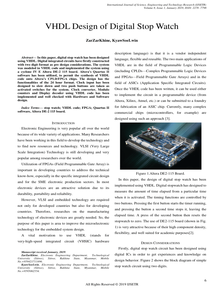
International Journal of Science, Engineering and Technology Research (IJSETR) Volume 8, Issue 1, January 2019, ISSN: 2278 -7798 VHDL Design of Digital Stop Watch ZarZarKhine, KyawSoeLwin description language) is that it is a vendor independent Abstract— In this paper, digital stop watch has been designed using VHDL. Digital integrated circuits have firstly constructed with two digit format as pre design considerations. The system was modeled in VHDL code and implemented the system using a cyclone IV E Altera DE-2 115 board. Altera’s Quartus II software has been utilized, to permit the synthesis of VHDL code onto Altera’s CPLD/FPGA chips. The design has the functionalities of the 24 hour format. Clock input has been designed to slow down and two push buttons are taken as activated switches for the system. Clock converter, Modulo counters and Display decoder using VHDL code has been implemented and well checked with Hardware and Software design. language, flexible and reusable. The two main applications of Index Terms— stop watch; VHDL code; FPGA; Quartus II software, Altera DE-2 115 board. for fabrication of an ASIC chip. Currently, many complex VHDL are in the field of Programmable Logic Devices (including CPLDs—Complex Programmable Logic Devices and FPGAs—Field Programmable Gate Arrays) and in the field of ASICs (Application Specific Integrated Circuits). Once the VHDL code has been written, it can be used either to implement the circuit in a programmable device (from Altera, Xilinx, Atmel, etc.) or can be submitted to a foundry commercial chips (microcontrollers, for example) are designed using such an approach [3]. INTRODUCTION Electronic Engineering is very popular all over the world because of its wide variety of applications. Many Researchers have been working in this field to develop the technology and to find new resources and technology. VLSI (Very Large Scale Integration) Technology is still developing and very popular among researchers over the world. Utilization of FPGAs (Field Programmable Gate Array) is important in developing countries to address the technical know-how, especially in the specific integrated circuit design and for the SME electronic production sectors. In most electronic devices are an attractive solution due to its However, VLSI and embedded technology are required not only for developed countries but also for developing countries. Therefore, researches on the manufacturing technology of electronic devices are greatly needed. So, the purpose of this paper is area to improve the microelectronic motivation to use implemented using VHDL. Digital stopwatch has designed to when it is activated. The timing functions are controlled by two buttons. Pressing the first button starts the timer running, and pressing the button a second time stops it, leaving the elapsed time. A press of the second button then resets the stopwatch to zero. The use of DE2-115 board (shown in Fig. 1) is very attractive because of their high component density, technology for the embedded system design. vital In this paper, the design of digital stop watch has been measure the amount of time elapsed from a particular time durability, portability and reliability. A Figure 1.Altera DE2-115 Board. VHDL (stands for flexibility, and well suited for academic purposes[2]. very-high-speed integrated circuit (VHSIC) hardware DESIGN CONSIDERATIONS Firstly, digital stop watch circuit has been designed using Manuscript received January, 2019. ZarZarKhine, Electronic Engineering University (Sittwe), Sittwe, Rakhine No.+959421711496. KyawSoeLwin, Electronic Engineering University (Sittwe), Sittwe, Rakhine No.+9595062554. Department, Technological State, Myanmar, Mobile digital ICs in order to get experiences and knowledge on Department, Technological State, Myanmar, Mobile stop watch circuit using two digits. design behavior. Figure 2 shows the block diagram of simple 6 All Rights Reserved © 2019 IJSETR International Journal of Science, Engineering and Technology Research (IJSETR) Volume 8, Issue 1, January 2019, ISSN: 2278 -7798 In this circuit a 555 timer IC is used as astable Figure 4 shows the experimental result of tested circuit. After multi-vibrator to make ‗1‘ second delay together with two having experiences and gained knowledge from the common cathode seven segment displays. The output of constructed digital circuit, VHDL design will be continued to astable multi-vibrator is directly applied to IC CD40110, carry out the system implementation. Up/Down counter, Latch and seven-segment decoding in one package IC is used and is very easy to interface with seven segment displays. This is fully static counter operational IC and ideal for low power displays. Figure 2.Block Diagram of simple stopwatch circuit Figure 4.Tested Circuit of simple stop watch circuit using This IC can be used for decade counting seven segment two displays decimal displays. One push button is used to stop/start the Now, it was found to be explained that is why needed to stopwatch and other push button is used to reset the use FPGA based system on chip design. Following section stopwatch. 5 volts is provided to this circuit to run this will be presented VHDL design with more functions, more stopwatch. Astable multi-vibrator generates one seconds displays and more efficient. Figure 5 shows state diagram and delay, this delay pulse of 0 and 1. This pulse was used for Figure 6 shows block diagram of system design. triggering the seven segment decoder. Reset U4 Start/ Pause CA SET J CA U1 Q COU N Upda T/ te Time U3 CLK VCC K 5V ~Q A B C D E FG A B C D E FG RESET JK_FF STOP START Reset 33kΩ R1 40110 Elap sed Time Clock 56kΩ R2 555_VIRTUAL Timer VCC RST 0.01µF C OUT Carry Clock DIS 40110 THR TRI Figure 5.State Diagram CON GND 1Hz clock signal Figure 3.Schematic diagram of simple stop watch circuit HH Counter using two displays M1 counter 0-5 Seven segment decoder changes the digit number with the one second of time period. When ON the stopwatch ( by When M1 is 0000 Clock pulse to HH M0 counter 0-9 S0 counter 0-9 When S1 is 0000 Clock pulse to M0 When M0 is 0000 Clock pulse to M1 S1 counter 0-5 When S0 is 0000 Clock pulse to S1 Binary to BCD Converter start/stop button), it start counting from zero and if turned OFF the same button then counting is stop or pause until B to 7S B to 7S Converter Converter again turned ON the same button or press reset button. There are two seven segments, so this stopwatch circuit can count H H B to 7S Converter M B to 7S Converter M B to 7S B to 7S Converter Converter S S Figure 6.Block diagram of system design 00-99 seconds time. Figure 3 shows schematic diagram and 7 All Rights Reserved © 2019 IJSETR International Journal of Science, Engineering and Technology Research (IJSETR) Volume 8, Issue 1, January 2019, ISSN: 2278 -7798 This is a structural model. It has 6 stages and each stage corresponds to one digit. There are three inputs to this system. The 50 MHz is connected to the internal clock. Start/stop and reset are mapped to the switches. The 50MHz internal clock will be slowed down to 1Hz, so the tenth second digit will increment at every rising edge of this clock. Since, it‘s a modulo 10 counter, once it hits 9, it will go back to 0. In addition, this counter will provide a 10 times slower clock (0.1Hz) to the next stage (second digit). Therefore, the second digits will increment every second. Applying the same idea to connect the other three stages in cascade, eventually, second and ten minute will be ten times slower than their previous stages. Each stage will provide one digit in 4-bit binary format. The outputs from the decoders will be mapped to their corresponding segments on the board. Essentially, each digit of digital stop watch is implemented as modulo counter. To be more specific, digits tenth second, second and minute are mod ‗9‘ counters because their values can only go from 0 to 9. Ten second, ten minute are mod 5 counters since their values can only go from 0 to 5. Digit tenth hour is mod 2 since mod 2 counters are using a single process(clk1) begin if(clk1'event and clk1='1') then count<= count+1; if(count = .; 25000000) then clk<= not clk; count<=1; end if; end if; end process; Therefore, the output clock will be 1Hz. The same mechanism will be applied for each stage to get proper clock speed. Because the clock is driving the entire system, so Start, Pause and Reset are also fed into the converter to control the clock. And all the push buttons on the Altera DE2 -115 are low active. Therefore, the values of Start, Stop, Pause and Reset need to be inverted before connect to other components. In order to display them on the LEDs, BCD -to-7 decoder has to be designed, which will decode each 4-bit digit into 7-bit display format. The following is the behavior of the decoder. Begin case LED_BCD is flip-flop can produce a count of 0 or 1, giving a maximum when ―0000‖, Leds_out<= ―0000001‖ ;--―0‖ count of 2 while the unit hour is mod 3 since it can only range when ―0001‖, Leds_out<= ―1001111‖ ;--―1‖ from 0 to 3. This also indicates that the maximum range of when ―0010‖, Leds_out<= ―0010010‖ ;--―2‖ this alarm clock is from 00:00:00 to 23:59:59. when ―0011‖, Leds_out<= ―0000110‖ ;--―3‖ 1) Clock converter and decoder design when ―0100‖, Leds_out<= ―1001100‖ ;--―4‖ In this section, clock converter and display decoder design when ―0101‖, Leds_out<= ―0100100‖ ;--―5‖ have been implemented with VHDL code to slow down the when ―0110‖, Leds_out<= ―0100000‖ ;--―6‖ master clock and to decode the display format. Altera DE2 when ―0111‖,Leds_out<= ―0001111‖ ;--―7‖ -115 Board with Cyclone IV FPGA is set to operate at a when ―1000‖, Leds_out<= ―0000000‖ ;--―8‖ frequency of 50MHz. This frequency cannot be used for when ―1001‖,Leds_out<= ―0000100‖ ;--―9‖ setting the timings in the digital clock, which is 5000000 when others, Leds_out<= ―- - - - - - -‖ times faster and so there is the need to reduce it to 1Hz. EN <= ―1111111‖ ; The 50MHz clock will be fed into the convert. Inside the converter, there is a counter driven by the rising edge of the 50M clock. When it counts from 0 to 2500000, it will invert the output clock and the counter will be reset to 0. At the end of the 50 million cycles, it sends a pulse to the remaining component parts. The variable count resets to 0 and the process continues. For Slow down the clock: Sevseg<= ; not (leds) ; end case; 2) Simulation and Experimental Results The FPGA used in the prototype is Development & Education Board DE2-115Altera‘s Cyclone IV E family. The code is written in VHDL and simulation software being used is Quartus II v7.2 software. Simulation result of stop watch design using Quartus II software has been shown in Figure 7. – 25000000 for one second (50MHz) 8 All Rights Reserved © 2019 IJSETR International Journal of Science, Engineering and Technology Research (IJSETR) Volume 8, Issue 1, January 2019, ISSN: 2278 -7798 By checking with initial simulation setup and running software, the system has been verified to provide evidence of the VHDL code. After that the result can been seen by extracting the additional outcomes with vector waveform file.Figure 8 shows the waveform simulation of system Consequently, digital stop watch can be useable and reliable. In this design, the adjustment of time function is not considered to simplify the digital system. The initial design considerations are more efficient for the first learner of the VHDL design. Modulo counters, decoders for display and clock converter are designed with VHDL. Hardware and software design are implemented as system expected. design. Finally, the digital stop watch using VHDL is ready to download on board of DE2-115. The tested results show in Figures 9. ACKNOWLEDGMENT First of all, the authors would like to express their special thanks to Dr. MyoTheinGyi, Union Minister of Education, the Republic of the Union of Myanmar, for his encouragement to do research works for regional development and applied science. The authors‘ grateful thanksgo to Dr. KyawHlaingOo, Acting Pro-Rector and Principal of Technological University (Sittwe) for his kind guidance, suggestion and directions throughout the preparation of research work, and valued motivations and encouragement as well. Finally, the authoris also sincerely thankful to our colleagues from the Departmentof Electronic Engineering,Technological University (Sittwe) offered strong moral and physical support. Figure 7.Quartus II simulation REFERENCES [1] Charles H. Roth, Jr., ―Digital System Design Using VHDL‖, PWS Publishing Company, 20 Park Plaza, Boston, 1998 [2] DE2-115 User Manual, 2003-2010, terasic technologies. Inc [3] Volnei A. Pedroni, ―Circuit Design with VHDL‖, MIT Press, Cambridge, Massachusetts, London, England, 2004 [4] Ian Grout, Digital System Design with FPGAs & CPLDs. ISBN-13: 978-0-7506-8397-5, United States, (2008). [5] Thomas L. Floyd, Digital Fundamentals, 9th Edition, Pearson International Edition, ISBN-0-13: 197255-3, Prentice Hall, (2006). [6] www.altera.com, Cyclone IV E hand-book.. Figure 8.Waveform simulation ZarZarKhine has received her B.E. degree in Electronic Engineering (in 2005) from Technological University (Sittwe), M.E. degree in Electronic Engineering (in 2010) from West Yangon Technological University. She is dedicated to teaching field from the last 13 years. She has supervised four under graduate students. Her research areas are electronic circuit design (including VHDL) and RF and Microwave Circuit Design. At present she is working as lecturer of Electronic Engineering Dept. at Technological University (Sittwe), Rakhine State, Myanmar. KyawSoeLwin has received his B.E. degree in Electronic Engineering (in 2002), M.E. degree in Electronic Engineering (in 2004) from Yangon Technological University and Ph.D. degree in Electronic Engineering (in 2009) from Mandalay Technological University. He is dedicated to teaching field from the last 16 years. He has supervised 25 M.E students, guided 5 Ph.D. students and 50 under graduate students. His research areas are power electronics, electronic circuit design (including VHDL) and RF and Microwave Circuit Design. At present he is working as Professor and Head of Electronic Engineering Dept. at Technological University (Sittwe), Rakhine State, Myanmar. Figure 9.Testing with DE2-115 The display is fully functional as expected design goals. The reset switch works when pressing the push buttons. CONCLUSION Digital stop watch has been designed using VHDL languages. It can be modified with more complex design to achieve in making seconds divider of tens or hundreds. 9 All Rights Reserved © 2019 IJSETR


